

Beyond Printed Electronics: A Smarter Layer
The Loomia Electronic Layer (LEL) is an award-winning soft circuit technology that delivers flexibility, durability, and design freedom that alternative approaches like printed electronics fall short of.
What are Printed Electronics?
Printed electronics are circuits formed by depositing conductive materials, such as conductive ink, onto a substrate. They emerged as a promising path toward flexible, lightweight electronics for wearables and next-generation devices.
Instead of etching away metal as in a traditional PCB, conductive patterns are printed or deposited, enabling thin, curved, and flexible configurations. But the technology comes with real tradeoffs in performance, integration, and scale.
Conductive Ink Printing
Silver or carbon-based inks are screen-printed or inkjet-deposited onto flexible substrates. Conductivity is limited, and curing processes can restrict material choices.
Substrate Limitations
Printed electronics often require smooth, uniform substrates. Direct application to textiles, leather, or complex 3D surfaces introduces significant adhesion and cracking challenges.
The Loomia Electronic Layer
The Loomia Electronic Layer takes a fundamentally different approach — assembling circuits within a layered TPU construction that bonds to virtually any surface without the fragility of printed traces.
Technology Comparison: Printed Electronics vs. the LEL
| Factor | Printed Electronics | Loomia Electronic Layer ✦ |
|---|---|---|
| Flexibility | Conductive inks can crack under repeated flexing and deformation | TPU construction flexes and stretches without trace failure |
| Multifunctionality | Typically single-function per layer; separate processes needed | Heating, lighting, sensing, switching — all in a single layer |
| Textile Integration | Inks don't adhere well to fibrous or porous surfaces | Sewable and thermally bondable into fabrics, leather, and soft goods |
| Customization | New printing masks required for shape or circuit changes | Freely customizable circuitry, shape, size, and connector placement |
| Durability | Ink traces degrade with washing, UV, and mechanical stress | Encapsulated within TPU — resistant to abrasion, moisture, and repeated cycles |
| Scalability | High initial tooling and setup costs | Scalable from prototype to production; modular design reduces NRE overhead |
| Prototyping Speed | Printing setup and substrate sourcing adds lead time | Rapid iteration with existing circuit libraries and modular components |
Printed Electronics Resources by Loomia
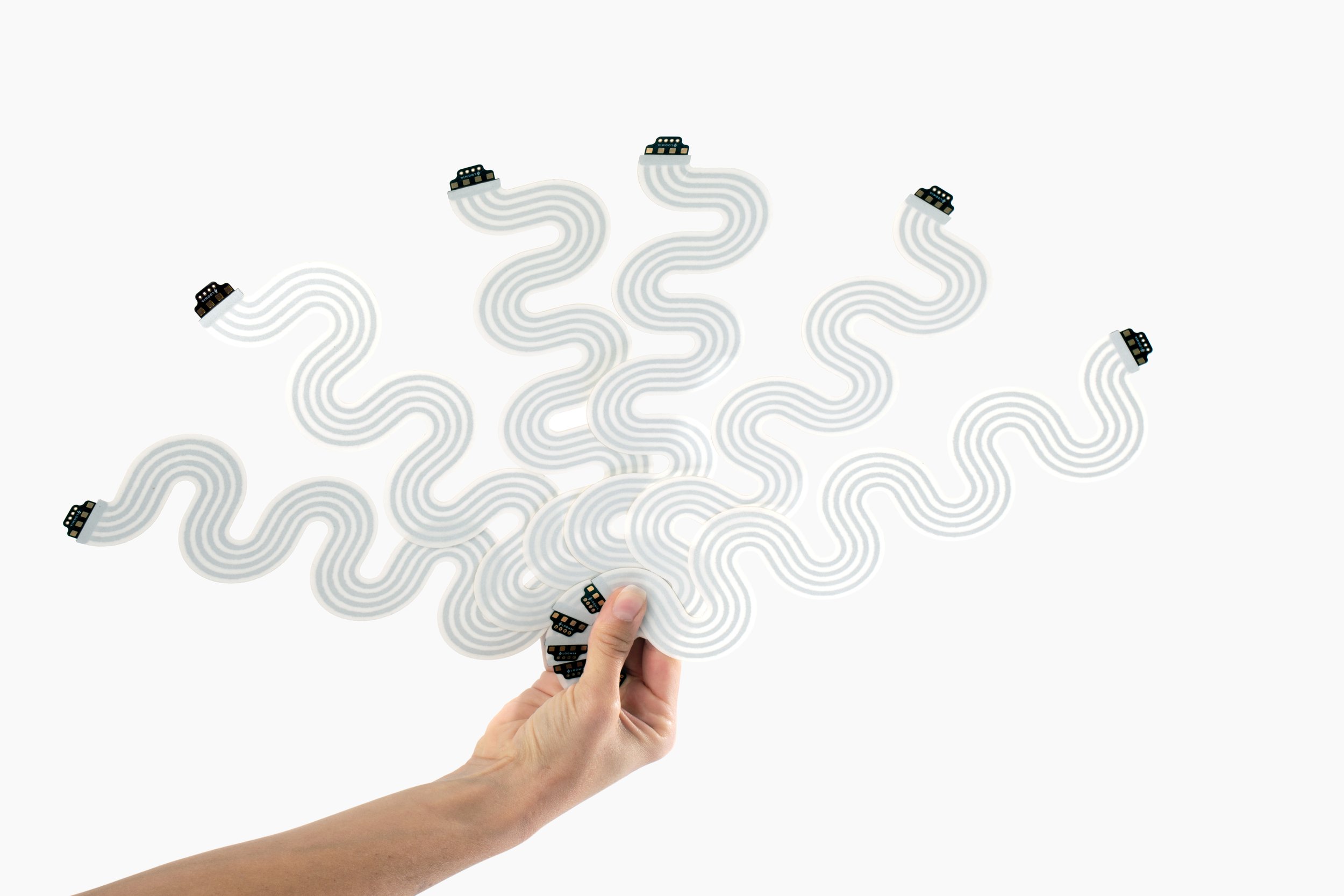
What Are Printed Electronics?
A quick overview of how printed electronics are shaping applications across wearables, automotive, and smart surfaces.
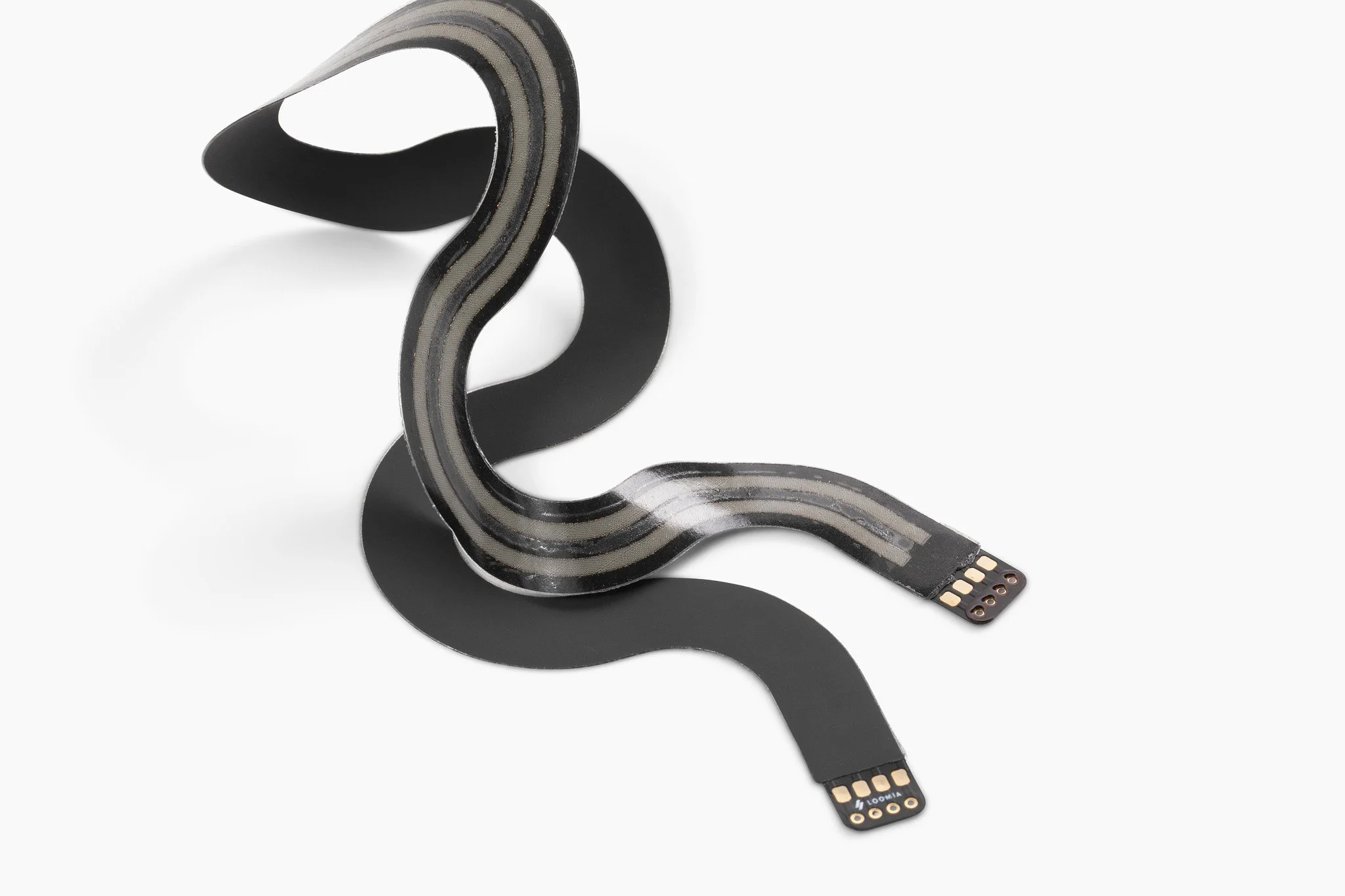
The LEL Vs. Printed Electronics
This article compares printed electronics with the LOOMIA Electronic Layer, looking at how each approach differs in flexibility, durability, and integration.
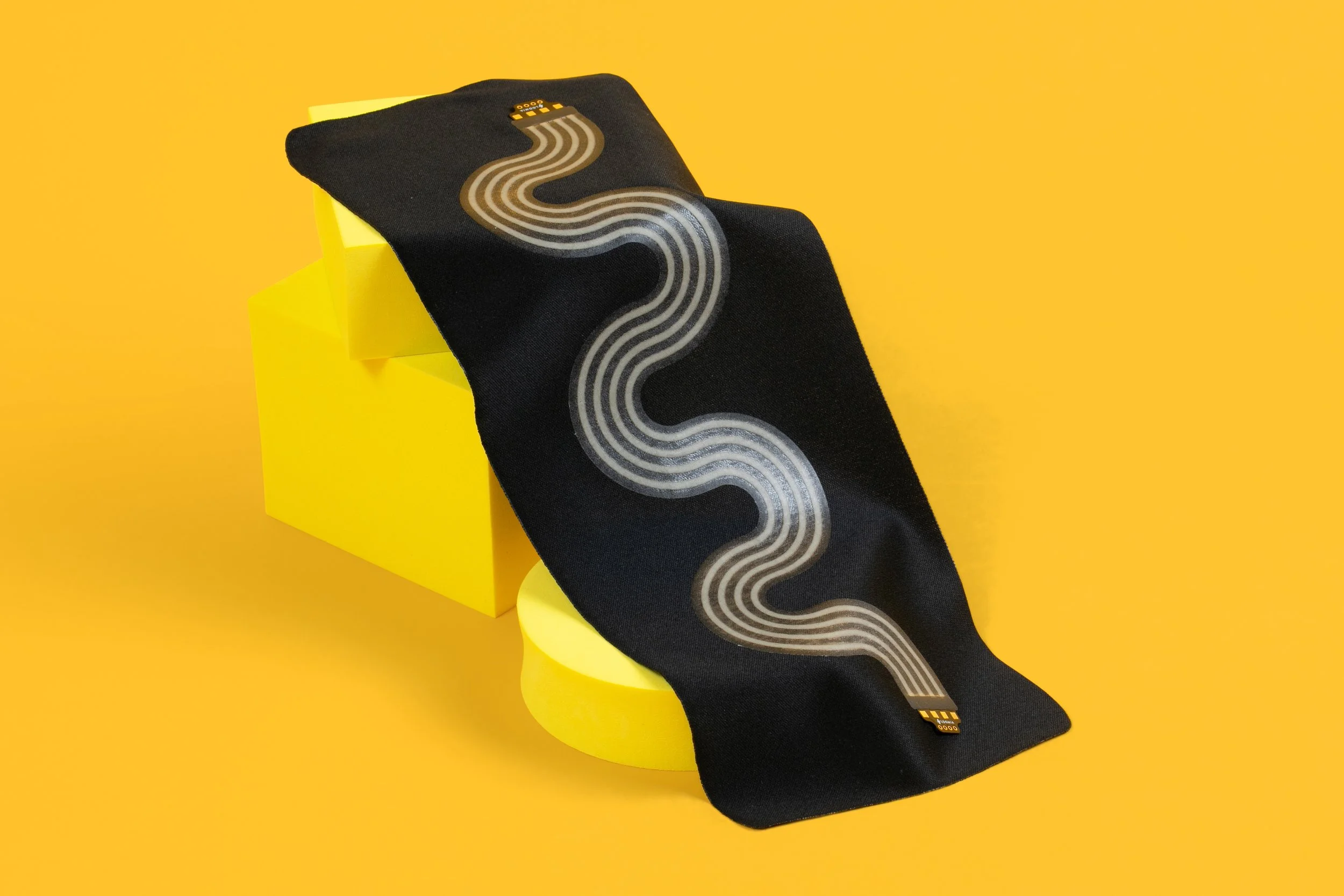
E-Textile vs. Printed Electronics Sustainability Analysis
Our team spent a year conducting a sustainability analysis on our material and collaborated with Sustainable Futures Lab to keep our reporting objective.